As the process tool becomes more sophisticated and complicated, fiber sensors with stable detection and easy installation are required. We offer a wide range of products with specific features suitable for wafer detection in the semiconductor manufacturing.
Application: Wafer Mapping
When picking wafers with a robot gripper, it is necessary to detect the number and position of wafers set in the FOUP to avoid reducing throughput by unnecessary movements. There is also a risk of damage the wafer when the robot gripper is inserted due to narrow wafer pitch or deflection of the wafer.
Our Solution: Fiber optics specific for wafer detection
OMRON offers sensors with specialized features that have a thin-profile head and are easy to mount on robot arms for semiconductor manufacturing applications.
OMRON offers solution support for wafer transfer in the semiconductor manufacturing, by utilizing the features of this sensor to detect the number and position of wafers in the FOUP with a retro-reflective sensor.
Enabling Technologies
Sensors designed specifically for reliable detection of wafers
Fiber sensors for wafer mapping have thin-profile and are easy to mount on robot arms. Optical axis adjustment is also easy. Fiber sensors for wafer reliably detect wafers even between stacked closely together.
Related Products
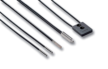
Precision detection fiber sensor heads
Highest precision in design and manufacturing of the fibers and focal lenses ensure highest beam and spot accuracy allowing the detection of smallest objects and height differences of less than 100 μm.
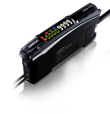
High-performance digital fiber amplifier
The E3NX-FA amplifier is best choice for most challenging fiber applications in terms of long sensing distance, minute object detection or high speed processes.

Smart Fiber Amplifier Units
2-channel Amplifier reduces installation space by half. Downsized Equipment and Control Panels
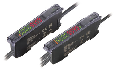
Smart Fiber Amplifier
The most cost-effective solution for a stable detection
Do you want to know more?
Contact Our Experts
Ota minuun yhteyttä Wafer Mapping

Kiitos yhteydenotostasi. Otamme teihin yhteyttä mahdollisimman pian.
Meillä on teknisiä ongelmia. Emme ole pystyneet vastaanottamaan lomakettasi. Pahoittelemme ja pyydämme yrittämään uudelleen myöhemmin.
Download